Block Diagram Of Balanced Modulator
Modulator dsb sc fet using balance Modulator equivalent carrier Balanced modulator circuit
Balance Modulator Using FET DSB-SC - YouTube
Ssb modulator under repository-circuits -32807- : next.gr Balanced modulator circuit diagram Modulator balanced explain
Generation of dsbsc signal using balanced and ring modulator
D.s.b. balanced modulatorModulator communication Angle modulation (am)Modulator balanced fet ssb circuit circuits full gr next above size click.
Modulator block diagram balanced carrier dsb sc signal sideband double suppressed explain generation system am figSolved the circuit shown below is known as a "balanced Ring modulatorAnalog communication.

(a) block diagram of a balanced modulator (b) mo-ccii based balanced
Engineering made easy: low level and high level modulation blockModulator diagram qpsk Modulator balanced schematicRing modulator for the double sideband suppressed carrier generation.
Modulator balanced using dsb sc generation diodes signal explain diode linear device non bridge fig electronicspostSolved explain how the balanced modulator shown in fig. p9.3 Balanced modulator notesModulation modulator balanced amplitude chapter ppt powerpoint presentation am signal slideserve.

Balanced modulator schematic diagram here bal installed components board 2004 jan updated click
Qpsk modulator : block diagram of modulatorModulator balanced adjustment balance Explain balanced modulator.Explain the generation of am waves using square law modulator and.
Block diagram of qpsk modulator.Modulator signal Modulator ring balanced signal frequency carrier vs am output unbalanced cancelling rm effect makes because different than hasQpsk modulator.

Analog communication
Schematic of balanced modulatorModulator switching generation explain Balanced modulator using transistorSolved 1. draw the modulator block diagram for am modulation.
Balance modulator using fet dsb-scDsb modulator balanced sideband suppressed fig genaration Introduction to double sideband suppressed carrier (dsb-sc) systemBalanced modulator circuit for dsb-sc am generation.

Solved problem 4: the block diagram for a modulator is
Modulator balanced transformer signal applied carrier primaryModulator balanced transistor using Fet balanced modulator for ssb under repository-circuits -53908- : next.grModulator balanced demodulator rf circuits suppressed carrier explanation schematics.
Explain the generation of dsb-sc signal with balanced modulator usingExplain balanced modulator Square law modulator, am modulation with block diagram and derivationLevel modulation diagram block high amplitude low am transmitter.

Lm1596 based balanced modulator circuit with explanation
Balance modulatorMore components are installed on the balanced modulator board. Balanced modulator transcribedIntroduction to double sideband suppressed carrier (dsb-sc) system.
Modulator balanced circuit .


Balanced Modulator Using Transistor - YouTube

Solved The circuit shown below is known as a "balanced | Chegg.com

Schematic of Balanced Modulator | Download Scientific Diagram

Solved Problem 4: The block diagram for a modulator is | Chegg.com
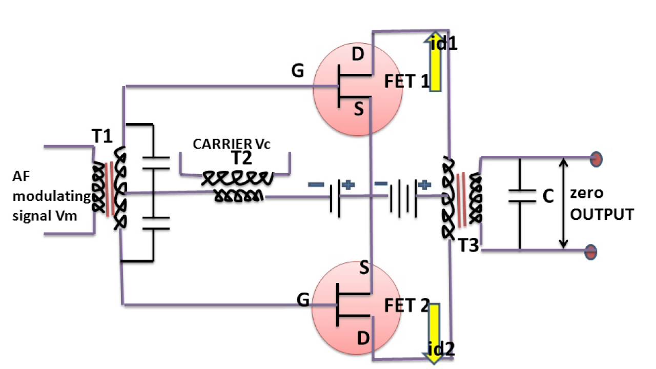
Balance Modulator Using FET DSB-SC - YouTube

Solved Explain how the balanced modulator shown in Fig. P9.3 | Chegg.com